
SEMVISION G3
EDX and Tilt Upgrade Available
0
nm
Resolution at 1 KeV
≥
0
Wafers per hour
≥
0
Defects per hour
0
nm
EDX Resolution
Applied Materials’ SEMVision G3 family, the industry’s fastest, most sensitive line of defect review and analysis tools for 65/45nm manufacturing and beyond. The new line of three systems sets the industry benchmark with 30nm sensitivity and throughputs of up to 1,800 defects per hour. Used in an optimized defect review strategy, these systems can accelerate customers’ production ramp by rapidly identifying the root cause of systematic and yield-limiting defects.
Get Quote
Learn More
The SEMVision product line includes the new Applied SEMVision G3 HP (high productivity) tool, the most productive system available for performing routine defect review and production process monitoring. The G3 HP provides a significant reduction in cost of ownership over previous tools, achieving world-class efficiency and lowest cost per defect.
The new Applied SEMVision G3 classic is the production workhorse system for volume defect review and material analysis, offering tilt and EDX(1) capabilities. As the ultimate system for inline root cause analysis, the recently introduced Applied SEMVision G3 FIB system, with integrated focused ion beam technology, provides complete capability for embedded defect and electrical failure analysis.
All three systems share the same proven platform, including the capability to share recipes, a common user interface and algorithms. This unique commonality shortens set-up time through extensive recipe sharing and provides high availability.
Applied’s SEMVision technology, which features industry innovations such as multi-perspective imaging, materials analysis and inline FIB, has rapidly expanded the use of SEMs(for defect analysis in manufacturing. The need for defect review has greatly increased and is now the third largest segment in the defect reduction market. Applied, with an installed base of nearly 700 SEMVision systems, is the leading supplier of this technology.
The new SEMVision family addresses the trend to achieve faster time to Resolution by harnessing the combined power of process and inspection expertise to dramatically cut the time and cost of resolving yield-limiting defects.
General Info
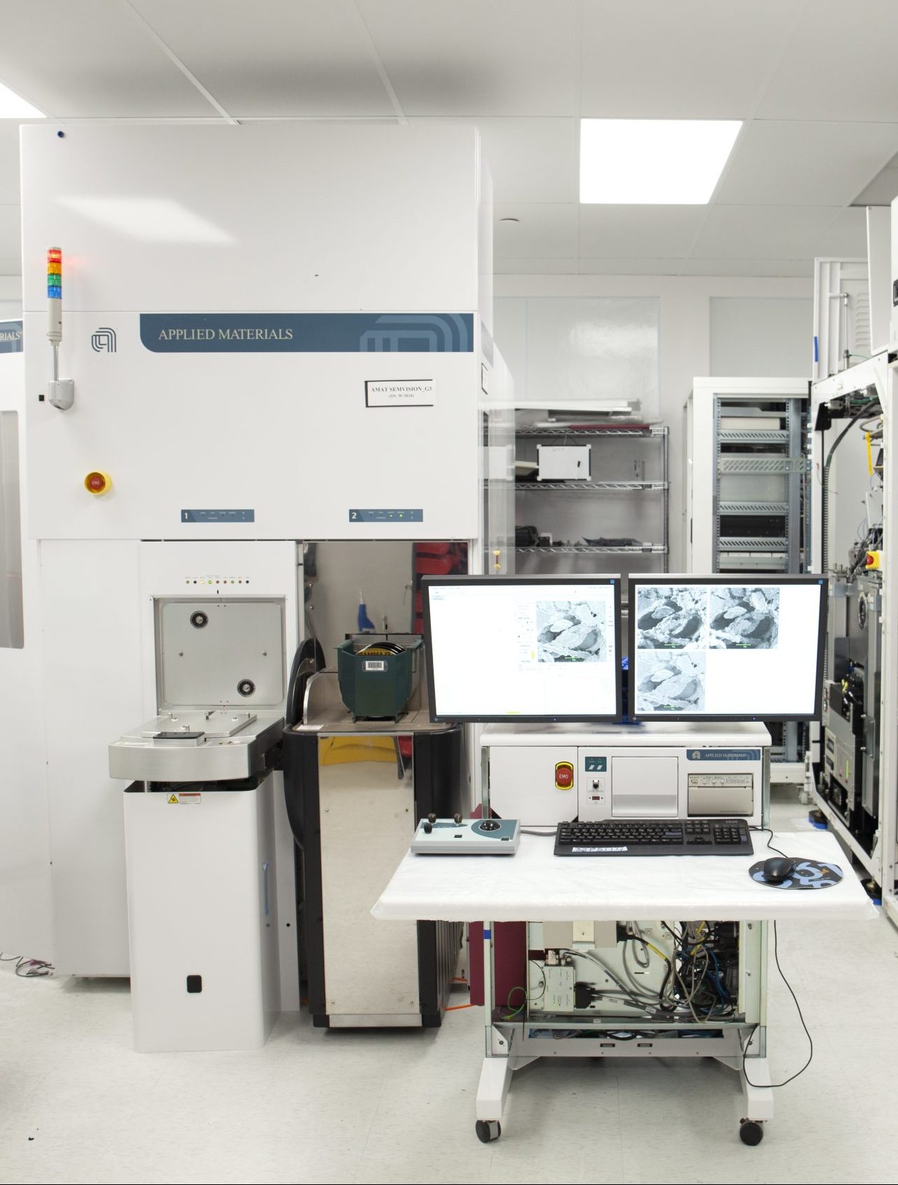
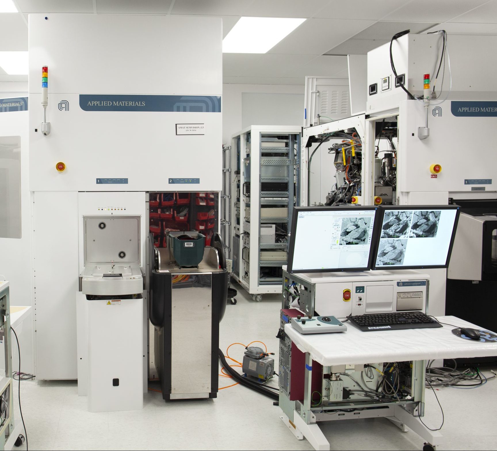
- Model: AMAT SEMVision G3
- Description: Defect Review System
- Wafer Size: 300mm
- Warranty: As Is or Refurbished to Customer Spec
Detail Configuration
- LoadPort Type: 2 Loadports with FOUP Capability
-
Loadport Maker: TDK
-
Carrier Reader: RFID type
-
Wafer System
Robot Maker: Brooks
Sight Source: SE-Gun Tip
Resolution: 4.0nm
Function
-
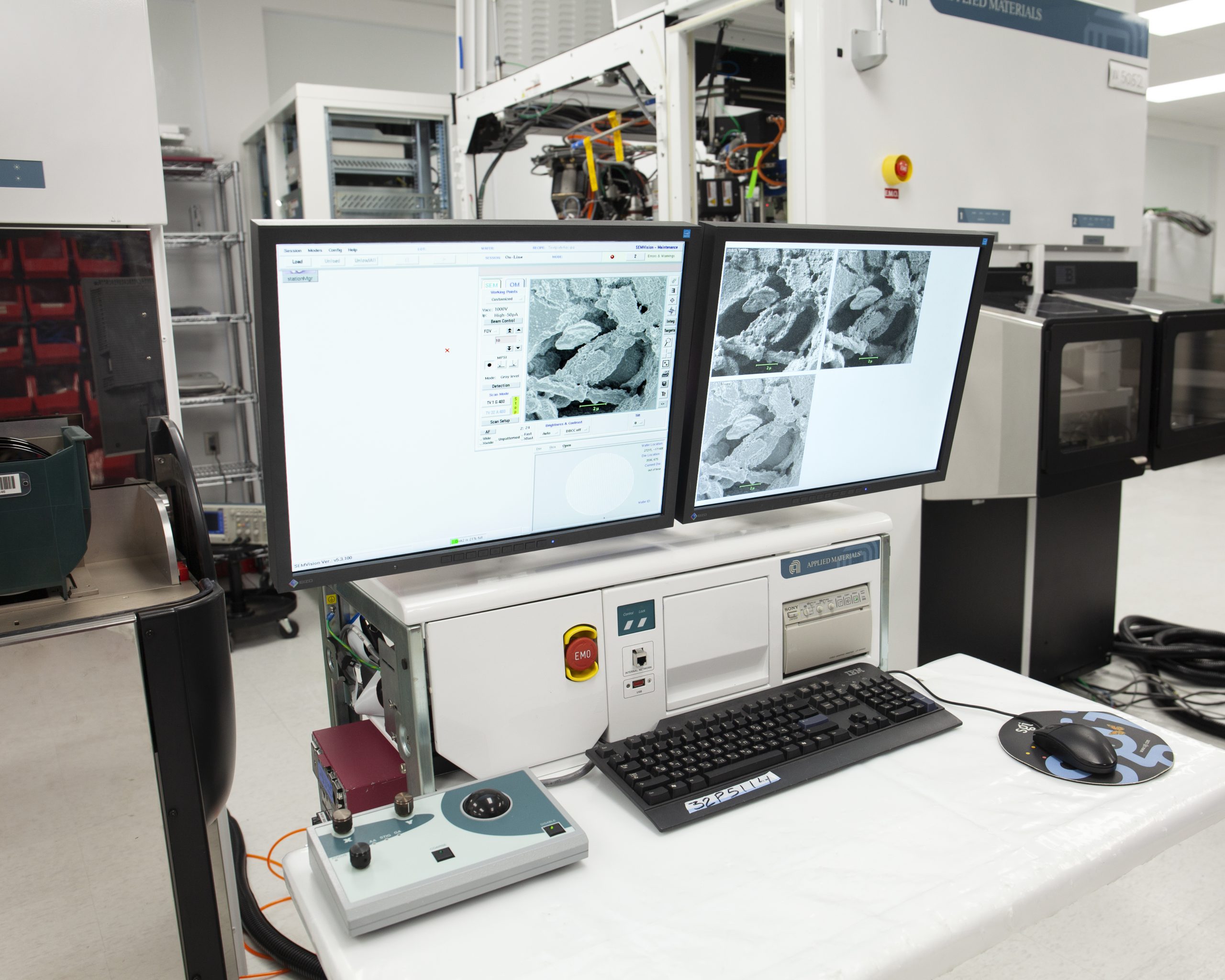
1. Optical Microscope
2. Automatic Defect Review
3. Automatic Defect Classification 4. Site Inspection
5. Automatic Defect Localization 6. Beam Tilt
7. EDX
Component
-
1. Main Unit
2. Operator Console 3. UPS
4. EPDU
5. FFU
6. Tool Cover
7. Isolation Block
Wafer Handling
Loader: AMAT ADO with RFID / OCLP / SMIF
Wafer Size: 300mm / 200mm
Configuration
FFU with ULPA Filter
SEM column
EDX column
45 Deg column Tilt
Wafer Rotation option included
Stage wafer holder ESC
ETU 300mm / 200mm
ITU 300mm / 200mm
Aligner
Optical Microscope X5 ,X20, X100
Software and Workstation
Software version
WS, IP/ODC SW, MEC, WHC): v5.4.500( latest version)
WorkStation SGI FULE
Software version (EDX): VTG_5.4.500 (latest version)
TFT LCD Monitors
IPU G3/G2
System performance
Pal (On the OTW, cassette / Slot 1: Delta X= 500 µms; Delta Y= 500 µm
ITU Repeatability: Delta X and Delta Y < 20 µm
Stage accuracy: Delta X and Delta Y < 1,5 µm
MTR: Delta X= 50; Delta Y= 30 µms
Specifications
Focus map / focus offset: 90% of the defect with Delta Z < 3 µms
Automatic defect offset/XY Map: 95% of the defects with Delta X < 1.5 µm and Delta Y < 1.5 µm
EDX resolution 4nm
Wafer throughput: 15 Wafers / Hours
Defects throughput: >1800 Defects / Hour
Cleanliness front side:
0.013 PWP / cm2 > size at 0.2 µm
Facility
Largest load ampere rating: 8 A
Full load current: 10 A
Interrupt current: 10,000 Amps I. C.
Supply voltage: 1-120 VAC, 1-Ph, 3-wires
208 V, 3-Ph, 5-wires, 50/60 Hz