
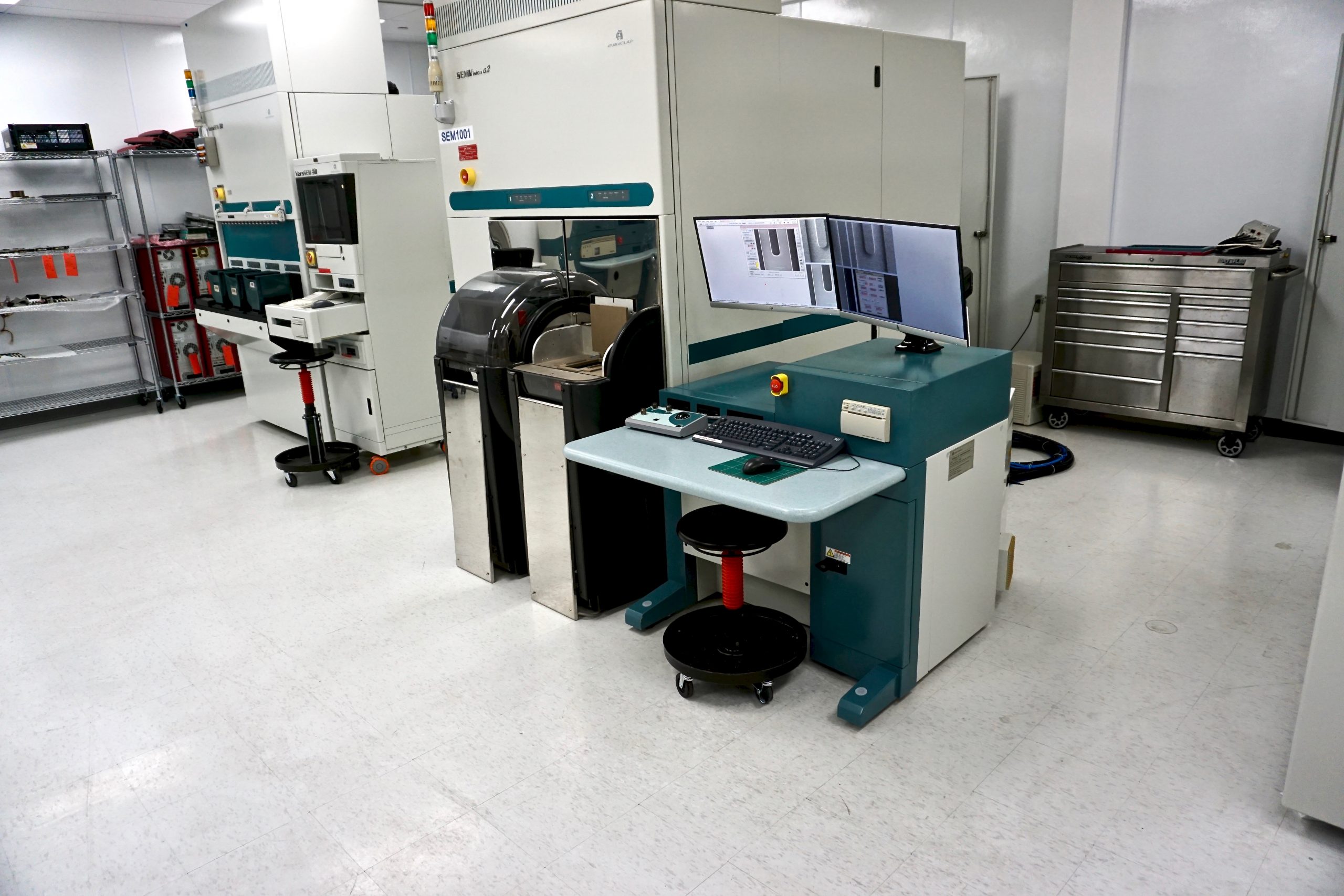
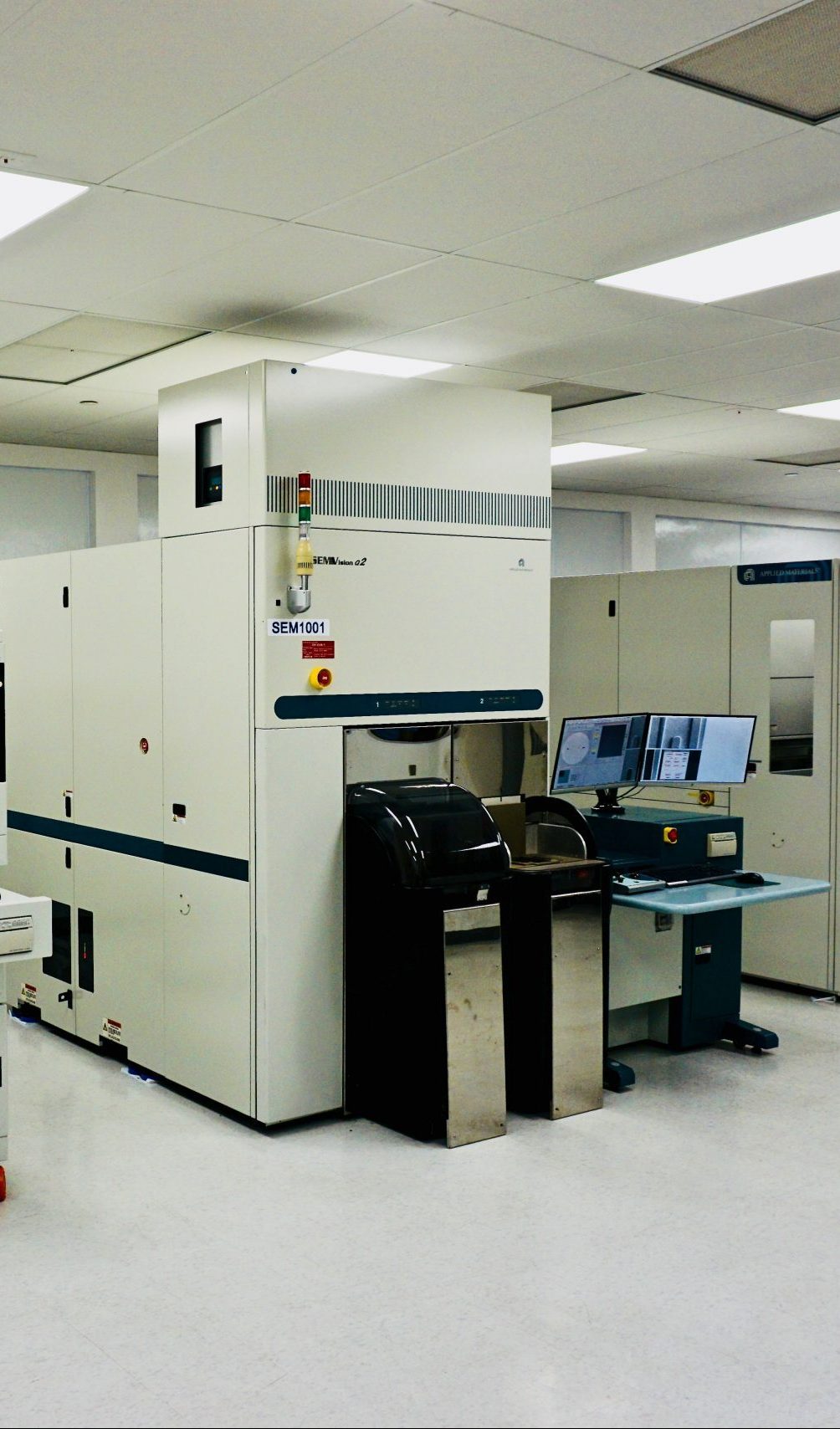
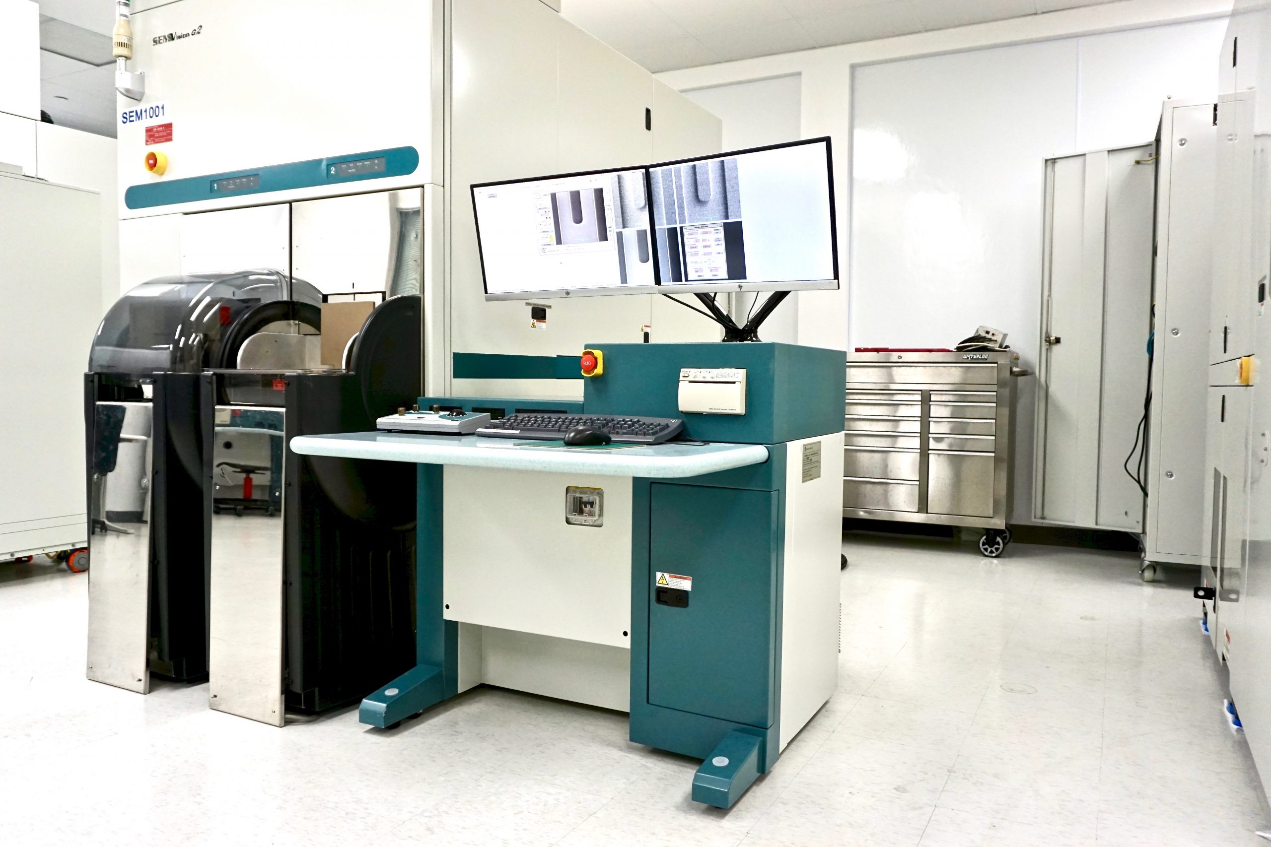
SEMVISION G2
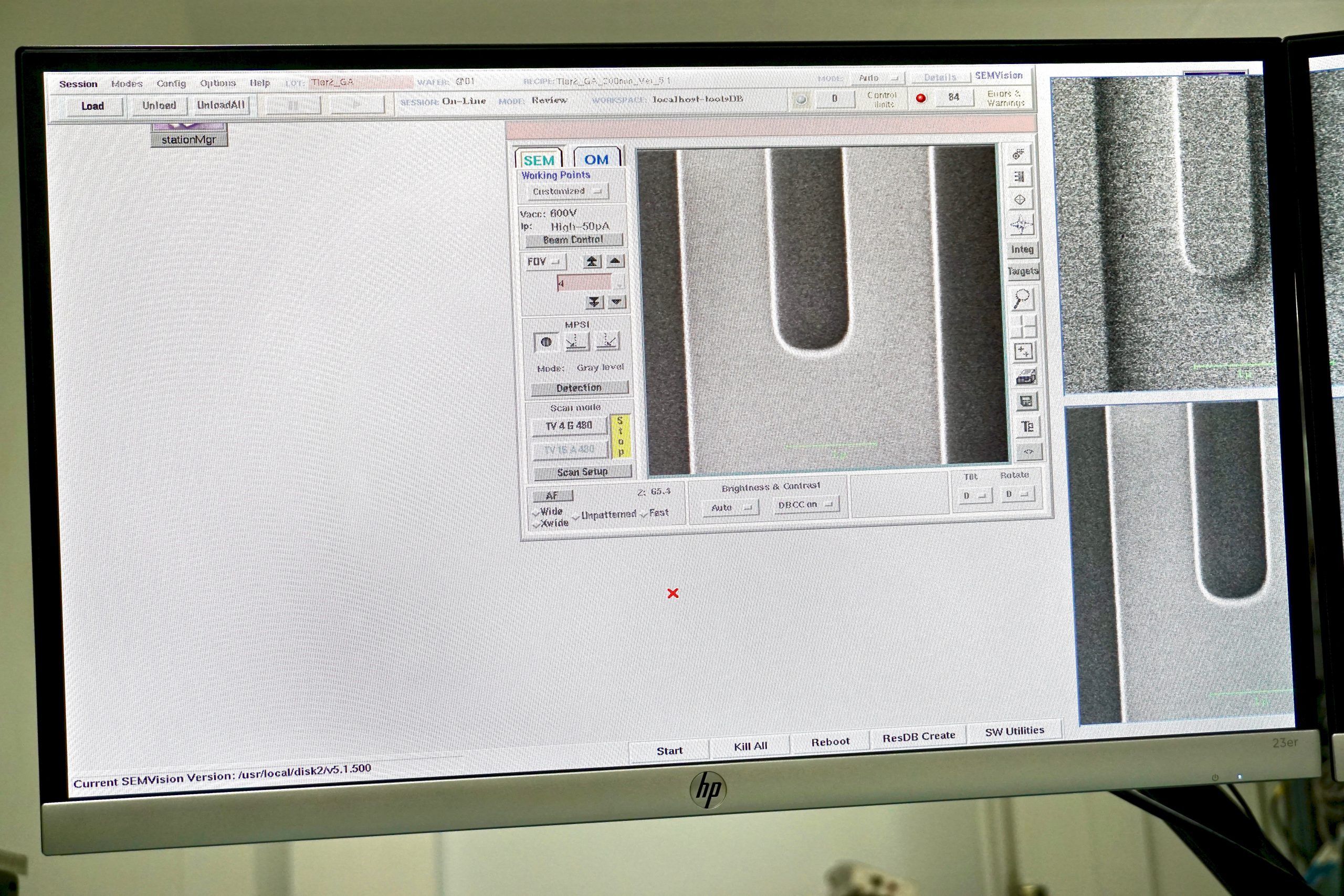
The SEMVision G2 ‘s detection assembly and processing make possible high-quality topographical images of tiny and shallow defects. High dynamic range detection, collection of back-scattered electrons, and energy filtering enable high aspect ratio imaging.
0
nm
Resolution at 1 KeV
≥
0
Wafers per hour
≥
0
Defects per hour
0
nm
EDX Resolution
General Info
- Model: AMAT SEMVision G2 +
- Description: Defect Review System
- Wafer Size: 300mm
- Serial Number: Multiple Systems Available
- Warranty: As Is or Refurbished to Customer Spec
Specifications
- Resolution at 1 KeV: 3 nm
- Focus map / focus offset: 90% of the defect with Delta Z < 3 μms
- Automatic defect offset/XY Map: 95% of the defects with Delta X < 1.5 μm and Delta Y < 1.5 μm
- EDX resolution: 4nm
- Wafer throughput: 12 Wafers / Hours
- Defects throughput: >1000 Defects / Hour
- Cleanliness front side: 0.013 PWP / cm2 > size at 0.2 μm
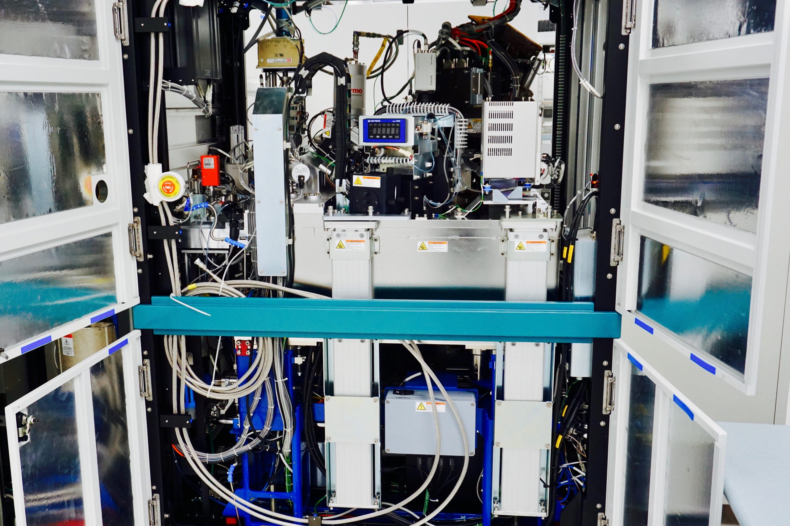
Configuration
- – FFU with ULPA Filter
- – SEM Column G2
- – EDX Column
- – 45 Deg Column Tilt
- – Wafer Rotation option included
- – Stage wafer holder 3 PIN
- – Aligner Optical Microscope X5, X20, X100
Wafer Handling
- Loader: AMAT ADO with RFID
- Wafer Size: 300mm
- ETU 300mm
- ITU 300mm
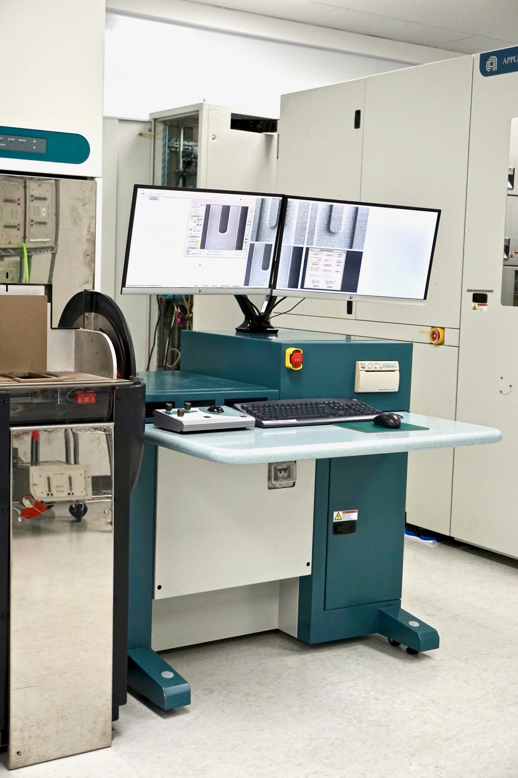
Software
- Software version (WS, IP/ODC SW, MEC, WHC): v5.1.500 WorkStation SGI FULE
- Software version (EDX): VTG_5.0.107
System Preformance
- Pal (On the OTW, cassette / Slot 1: Delta X= 500 μm; Delta Y= 500 μm
- ITU Repeatability: Delta X and Delta Y < 20 μm
- Stage accuracy: Delta X and Delta Y < 1.5 μm
- MTR: Delta X= 50; Delta Y= 30 μm
Facility
- Largest load ampere rating: 8 A
- Full load current: 10 A
- Interrupt current: 10,000 Amps I. C.
- Supply voltage: 1-120 VAC, 1-Ph, 3-wires 208 V, 3-Ph, 5-wires, 50/60 Hz